Scanning Electron Microscopes
Hitachi S-4800 FEG-SEM is optimised for high resolution (down to the nanometre range).
This equipment is designed to cover high magnification imaging needs on all types of materials. It is also used for the observation of fragile materials under the electron beam, such as biological samples, polymers, semiconductors or more generally materials or structures associated with nanotechnologies. The presence of a STEM (Scanning Transmission Electron Microscopy) detector extends the imaging capabilities of the SEM by giving access to certain information normally only accessible in a Transmission Electron Microscope (TEM).
Technical speficiations:
- field emission gun (cold cathode) : very high gun brightness
- wide range of acceleration voltages : from 0,1 kV to 30 kV
- guaranteed on-site resolution of 1 nm at 15 kV
- samples up to 40 mm in diameter
- SE/BSE images
- EDS analyses
- STEM detector
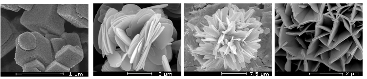
Application examples:
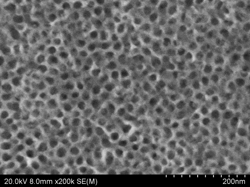
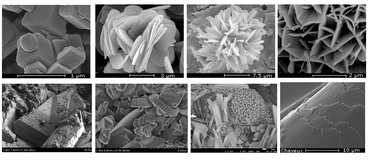
Nanopores (10-20 nm) in anodized aluminum (non coated)
Biominerals in roots
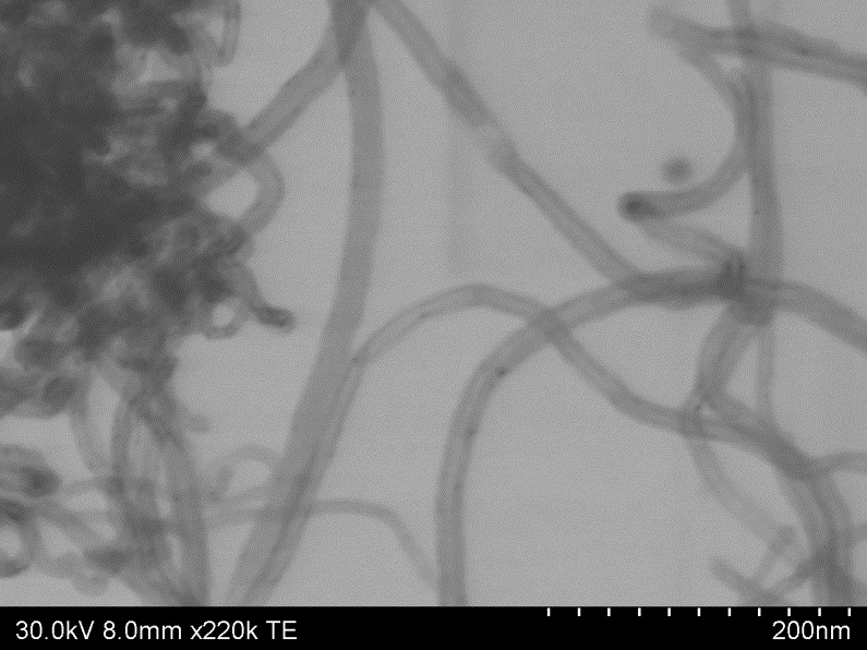
Carbon nanotubes (STEM)
JEOL J7600F FEG-SEM is dedicated to EDS/WDS analysis.
It is equipped with a coupled system consisting of a SDD-type energy-dispersive spectrometer (EDS) and an inclined wavelength-dispersive spectrometer (WDS).
This microscope allows observation and quantitative analysis (calibration standards) of polished samples (thin sections or polished sections) with very good resolution and high beam current (up to 200 nA at 30kV). It is also possible to acquire quantitative X-ray maps. Coupling with a WDS allows to remove some interferences due to the low spectral resolution of the EDS and to improve the detection limit.
Technical specifications:
- Schottky-FEG (high beam current, up to 200 nA)
- wide range of acceleration voltages : from 0,1 kV to 30 kV
- guaranteed on-site resolution of 1 nm at 15 kV
- samples up to 70 mm in diameter
- SE : In-lens upper secondary electron detector (SEI), Lower secondary electron detector (LEI)
- BSE : retractable BSE and LABE (Low Angle BE Detector) for high magnifications
- 20mm2 Oxford Instruments EDS
- Oxford Wave WDS
Application examples:
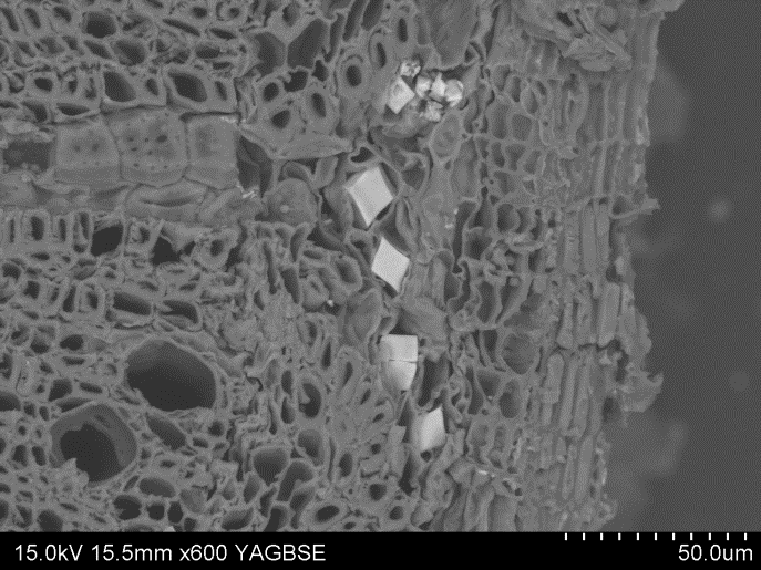
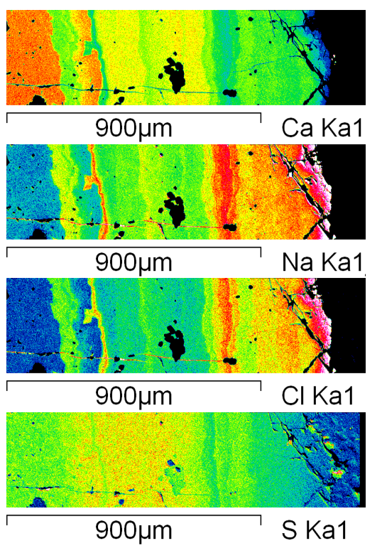
X-ray maps in a scapolite
TESCAN VEGA3 LM conventional SEM is dedicated to the observation and analysis of various types of samples, with or without coating, thanks to the possibility of working under low vacuum.
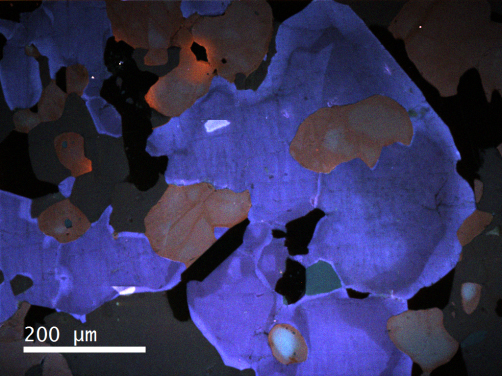
It is an easy-to-use equipment that is accessible on a self-service basis after specific training by authorized personnel. It is also equipped with a cathodoluminescence detector that allows the observation of textures in minerals that are usually impossible to obtain with standard optical or electron microscopy. Cathodoluminescence is also commonly used in the field of semiconductors, in particular to reveal various structural defects. It is possible to work under low vacuum (up to 500 Pa).
Technical specifications:
- tungsten filament gun
- guaranteed on-site resolution of 3 nm at 30 kV
- samples up to 80 mm in diameter
- low vacuum mode (up to 150 Pa or 500 Pa with a different diaphragm)
- SE/BSE images
- 30mm2 Bruker XFlash6 EDS
- Gatan ChromaCL2UV cathodoluminescence detector
Application examples:
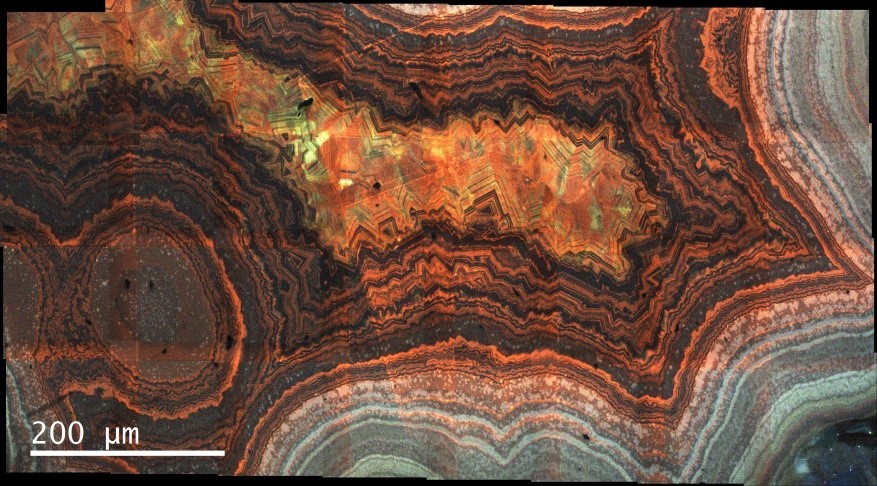
Cathodoluminescence of a quartz geode
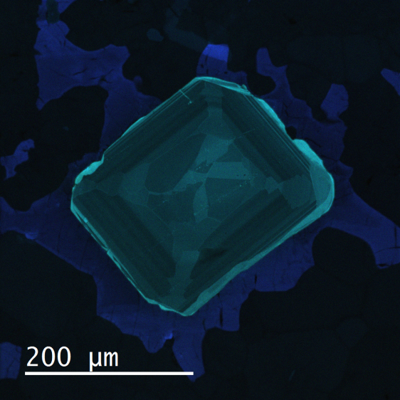
Cathodoluminescence of a zircon
Cathodoluminescence of a scapolite